
Most Popular
-
1
10-man S. Korea lose to Indonesia to miss out on Paris Olympic football qualification

-
2
Hybe-Ador feud should have limited effect on Hybe's overall performance: analysts

-
3
Second Gimpo civil servant found dead, after apologizing for not finishing work

-
4
DP leader says he will meet Yoon without conditions

-
5
First-ever meeting of president, opposition chief set to finally happen


-
6
NewJeans' singles, Japanese debut to proceed as planned, despite Hybe-Ador feud

-
7
Experts raise concerns about Japan putting pressure on Naver over Line

-
8
Samsung mobile chief, Google device head meet in Seoul

-
9
Blinken calls on China to press N. Korea to end its 'dangerous' behavior

-
10
Ship linked to NK arms shipments to Russia is moored in China: State Dept.


SK hynix unveils world’s first 321-layer NAND
With mass production set to start in 2025, Korean chip giant vows to solidify NAND leadership
By Jo He-rimPublished : Aug. 9, 2023 - 16:21
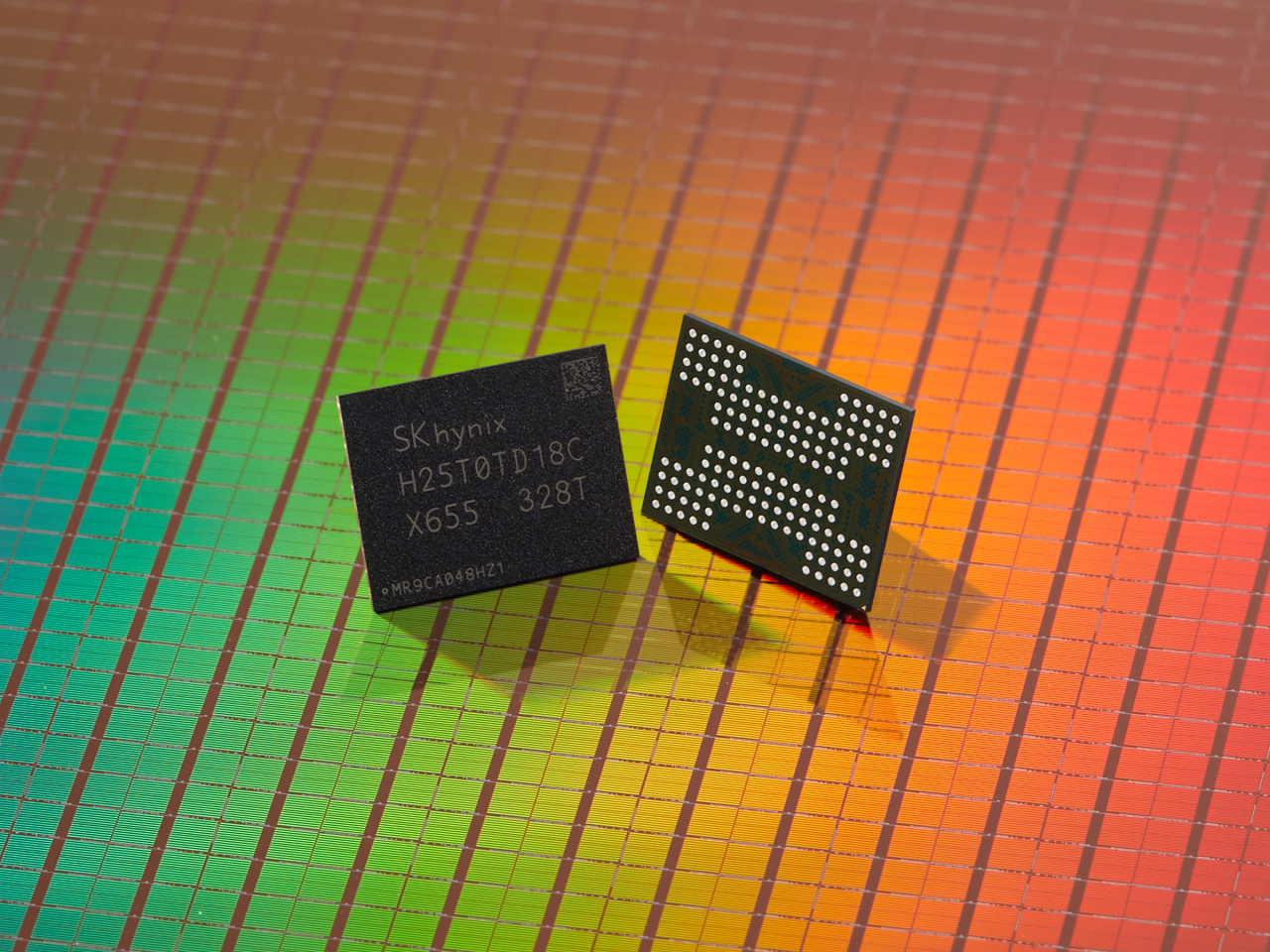
SK hynix, the world’s second-largest memory chip maker, unveiled samples of the world’s first 321-layer NAND and next-generation memory solutions for AI demand at a global industry conference in the US on Wednesday.
At the Flash Memory Summit, the world’s biggest annual conference for the NAND flash industry running from Tuesday to Thursday, SK hynix showcased its latest NAND flash chips and made public the progress on its development of the industry’s first NAND with more than 300 layers.
“With timely introduction of the high-performance and high-capacity NAND, we will strive to meet the requirements of the AI era and continue to lead innovation,” Choi Jung-dal, Head of NAND Development at SK hynix said in his keynote speech at the conference.
Choi added the company expects the ongoing development of the 321-layer product, the fifth generation of the 4D NAND, to help the company solidify its technological leadership in the NAND industry.
The firm's 321-layer chip in development is a 1 terabit Triple Level Cell 4D NAND flash. NAND flash products are categorized into single, multi, triple, quadruple and penta level cells depending on the number of information (in bit units) contained in a single cell. When a cell contains more information, it means more data can be stored within the same extent of area.
Revealing the detailed progress on the development, SK hynix said it will raise the level of completion of the 321-layer product and start mass production from the first half of 2025.
The move comes as the company seeks to maintain its market share, while the global memory chip market is expected to gradually recover from a severe downturn in the coming months.
According to SK, the 321-layer 1Tb TLC NAND comes with a 59 percent improvement in productivity compared to the earlier generation of 238-layer 512G. This is possible with the technology enabling stacking of more cells and larger storage capacity on a single chip to increase the total capacity produced by a single wafer, the company explained.
“With another breakthrough to address stacking limitations, SK hynix will open the era of NAND with more than 300 layers and lead the market,” the chipmaker said, explaining its success in producing the 238-layer NAND has helped the smooth progress for the development of the 321-layer product.
Since the introduction of ChatGPT, which accelerated the growth of the generative AI market, demand for high-performance and high-capacity memory products that can process more data at a faster pace is growing rapidly.
To meet the new demand, SK hynix also introduced next-generation NAND solutions optimized for such AI demand, including the enterprise SSD adopting the PCIe Gen5 interface and UFS 4.0.
The company said it expects these products to achieve industry-leading performance to fully meet the needs of the customers with a focus on high performance.
SK hynix also announced that it has started development of the next-generation PCIe Gen6 and UFS 5.0 with improved technology for solution development that it acquired through these products, and expressed its commitment to being a leading trendsetter in the industry.