
Most Popular
-
1
10-man S. Korea lose to Indonesia to miss out on Paris Olympic football qualification

-
2
Hybe-Ador feud should have limited effect on Hybe's overall performance: analysts

-
3
Second Gimpo civil servant found dead, after apologizing for not finishing work

-
4
DP leader says he will meet Yoon without conditions

-
5
First-ever meeting of president, opposition chief set to finally happen


-
6
NewJeans' singles, Japanese debut to proceed as planned, despite Hybe-Ador feud

-
7
Blinken calls on China to press N. Korea to end its 'dangerous' behavior

-
8
Experts raise concerns about Japan putting pressure on Naver over Line

-
9
Samsung mobile chief, Google device head meet in Seoul

-
10
Ship linked to NK arms shipments to Russia is moored in China: State Dept.


Samsung eyes AI chip leadership with highest-capacity HBM3E
Mass production slated for first half
By Jo He-rimPublished : Feb. 27, 2024 - 16:08
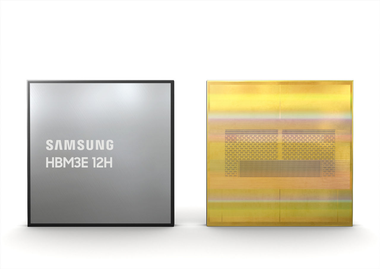
Samsung Electronics said Tuesday it has developed HBM3E 12H, the industry’s first 12-stack HBM3E DRAM and the highest-capacity HBM product to date, going one step further than its rivals in the burgeoning artificial intelligence chip market.
The world's largest memory chip maker said it has begun providing samples of HBM3E 12H to customers, and mass production is slated for the first half of this year.
“The industry’s AI service providers are increasingly requiring HBM with higher capacity, and our new HBM3E 12H product has been designed to answer that need,” Bae Yong-cheol, Executive Vice President of Memory Product Planning at Samsung Electronics said.
“This new memory solution forms part of our drive toward developing core technologies for high-stack HBM and providing technological leadership for the high-capacity HBM market in the AI era," he said.
High Bandwidth Memory is a memory chip with low power consumption and ultra-wide communication lanes, using vertically stacked memory chips to break processing bottlenecks caused by conventional memory chips.
In light of the exponential growth of the AI market, the advanced, high-capacity memory chip would be an optimal solution for future systems that require more memory, Samsung said.
When used in AI applications, it is estimated that, in comparison to adopting HBM3 8H, the average speed for AI training can be increased by 34 percent while the number of simultaneous users of inference services can be expanded more than 11.5 times.
"Its higher performance and capacity will especially allow customers to manage their resources more flexibly and reduce the total cost of ownership for data centers," Samsung said.
Samsung’s HBM3E 12H provides an all-time high bandwidth of up to 1,280 gigabytes per second (GB/s) and an industry-leading capacity of 36 GB, the company said. In comparison to the 8-stack HBM3 8H, both aspects have improved by more than 50 percent.
The HBM3E 12H applies advanced thermal compression non-conductive film (TC NCF), allowing the 12-layer products to have the same height specification as 8-layer ones to meet current HBM package requirements.
As the industry seeks to mitigate chip die warping that comes with thinner die, this technology is anticipated to have added benefits, especially for higher stacks, Samsung explained.
With its continued effort to lower the thickness of its NCF material, it achieved the industry's smallest gap between chips at seven micrometers, and also eliminated voids between layers, Samsung said. This has led to enhanced vertical density by over 20 percent when compared to the HBM3 8H, the chipmaker added.
Global chipmakers are seen competing to gain an upper hand in the HBM market, quickly gaining demand amid the increasing use of generative AI.
Micron Technology, a US-based chipmaker, announced it has started mass production of HBM3E, ahead of rivals Samsung and SK hynix. With a capacity of 24 GB, Micron's latest chip would be part of Nvidia's H200 Tensor Core GPUs, the company said.
The HBM market, which took about 1 percent of the total memory chip market in terms of volume last year, is anticipated to more than double this year.
Samsung Electronics and SK hynix are competing head-on to beat each other in the new chip market, each taking some 45 percent of the market share. Micron comes in at third on the list, supplying about 10 percent of all orders.